 |
| Silicon is a gray , brittle, tetravalent, nonmetallic element occurring abundantly in nature. Next to Oxygen it is the chief elementary constituent of the earth's crust. The symbol for Silicon is Si it's atomic number is 14 and it's atomic mass is 28.086. This element is almost always found in various compounds both in nature and in industry, in nature you find it in quartz, jasper, agate, flint, common beach sand, sandstone and many other common rocks and materials. In industry we find it as the main component in the most common building materials such as cement, bricks, glass and others. It is also used in many polymers such as Silicone rubber as well as thousands of other uses including heat resisting resins, lubricants, water resistant films etc., etc.Silicon as a Semiconductor: Perhaps one of the most important uses for Silicon in the second half of the twentieth century and beyond, is it's ability to conduct electricity in a very controlled manner. Relative to how many impurities or dopants (Boron, Phosphorus, Arsenic, Antimony, etc.) are placed into it's crystal structure. Simply put, the more dopant in the crystal lattice of Silicon the more it will conduct electricity. In theory pure monocrystalline Silicon will not conduct electricity very well at all, the beauty of Silicon is that it can be made to take on dopants precisely and after this doping it will normally remain stable under many adverse conditions. Thus making the Silicon wafer an ideal Palette or surface for the construction of today's and tomorrow's most advanced semiconductor devices. The making of a Silicon wafer: With all this talk of sand and glass it may begin to over simplify a very complex process. The process of growing Ingots of monocrystalline Silicon with a uniform and controlled dopant and oxygen content, and then to take these Ingots and grind, slice and polish them into the final Prime wafers mostly free of defects that major Fab's will use to build advanced semiconductor devices on, is nothing short of a monumental task. At Process Specialties we don't think that The Silicon Manufacturers will ever get enough credit for the work and the achievements they have made in helping to forward this industry to the place it is today. |
Raw Material: Silicon is the raw material of course, the crucible at the right is filled with pure 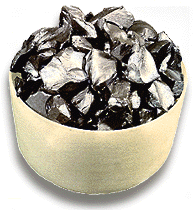 Polysilicon chips. These chunks of Poly have been made from sand by means of a complex reduction and purification process using Trichlorosilane and Hydrogen. Then the Polysilicon is further distilled and reduced and finally deposited on heated Titanium or Tantalum tubes. After further processing it becomes the material you see at the RIGHT or it may be in a granular form. The Poly is in a quartz container called a crucible and this material is now ready to go on to the next processing step in the manufacturing of a high quality Silicon wafer. This part of the manufacturing process is carried out by large Silicon manufacturers or the material is sometimes purchased by Silicon companies from other vendors. Polysilicon chips. These chunks of Poly have been made from sand by means of a complex reduction and purification process using Trichlorosilane and Hydrogen. Then the Polysilicon is further distilled and reduced and finally deposited on heated Titanium or Tantalum tubes. After further processing it becomes the material you see at the RIGHT or it may be in a granular form. The Poly is in a quartz container called a crucible and this material is now ready to go on to the next processing step in the manufacturing of a high quality Silicon wafer. This part of the manufacturing process is carried out by large Silicon manufacturers or the material is sometimes purchased by Silicon companies from other vendors. |
...Crystal Pulling is the next step in the Manufacturing of a Silicon wafer. In this process the Polysilicon chunks or granules are loaded into the Quartz crucible of the Crystal pulling furnace along with a small amount of either Boron, Phosphorus, Arsenic or Antimony dopant. The Polysilicon is 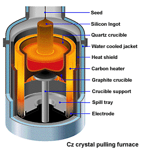 then melted at a process temperature of 1400° C in a high purity Argon gas ambient. Once the proper "melt " is achieved a "seed" of single crystal Silicon is lowered into the melt. Then the temperature is adjusted and the seed is rotated as it is slowly pulled out of the molten Silicon. The surface tension between the seed and the molten Silicon causes a small amount to rise with the seed, as it is pulled and cooled into a perfect monocystalline ingot with the same crystal orientation as the seed. The cut-away view at the LEFT is of the lower portion of the crystal pulling furnace, these machines can stand 12-15 feet high and are quite complex in nature. These furnaces also must be very stable and vibration free since the process takes hours and the slightest jarring of the furnace can break the Ingot from the seed. then melted at a process temperature of 1400° C in a high purity Argon gas ambient. Once the proper "melt " is achieved a "seed" of single crystal Silicon is lowered into the melt. Then the temperature is adjusted and the seed is rotated as it is slowly pulled out of the molten Silicon. The surface tension between the seed and the molten Silicon causes a small amount to rise with the seed, as it is pulled and cooled into a perfect monocystalline ingot with the same crystal orientation as the seed. The cut-away view at the LEFT is of the lower portion of the crystal pulling furnace, these machines can stand 12-15 feet high and are quite complex in nature. These furnaces also must be very stable and vibration free since the process takes hours and the slightest jarring of the furnace can break the Ingot from the seed. |
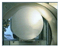
At the right is an actual picture of a "Seed" and Ingot inside of a crystal pulling furnace. 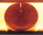 |
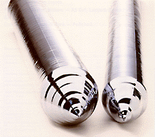 ...Next the finished Ingot is ground to a rough size diameter (a little larger than a finished wafer) and it is either notched or flatted along it's length to indicate the orientation of the Ingot. This is also a point when many inspections are made on the ingot to catch any major flaws or problems with resistivity etc. The 200mm and 150mm ingots at the LEFT are freshly pulled and have not yet been ground, notched or flatted. ...Next the finished Ingot is ground to a rough size diameter (a little larger than a finished wafer) and it is either notched or flatted along it's length to indicate the orientation of the Ingot. This is also a point when many inspections are made on the ingot to catch any major flaws or problems with resistivity etc. The 200mm and 150mm ingots at the LEFT are freshly pulled and have not yet been ground, notched or flatted. |
. Slicing: In the next step the Ingots are sliced into wafers using a diamond ID saw or other type of saw. Deionized water is used to cool the blade on this ID (inside diameter) saw. The saw at the RIGHT is slicing 150mm wafers and if you look closely you can see the major flat of the wafer on the left. Slicing: In the next step the Ingots are sliced into wafers using a diamond ID saw or other type of saw. Deionized water is used to cool the blade on this ID (inside diameter) saw. The saw at the RIGHT is slicing 150mm wafers and if you look closely you can see the major flat of the wafer on the left. |
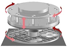 .Lapping is next, in this step the Ingots have now become rough cut Silicon wafers with saw marks and other defects on both sides of the wafer. Also at this point the wafer is much thicker than it will be when it is finished. Lapping the wafers accomplishes several things, it removes saw marks and surface defects from the front and backside of the wafers, it thins the wafer and relieves a lot of the stress accumulated in the wafer from the sawing process. Both before and after the lapping process many in-process checks will be done on the Silicon wafers and more fall-out will occur (good news for the people that need coin roll for test wafers). At the LEFT you can see a drawing of the "business end" of a typical lapping machine. After lapping the wafers go thru several cleaning /etching steps using sodium hydroxide or acetic and nitric acids to remove microscopic cracks and surface damage caused by the lapping process, this is followed by followed by deionized water rinses. .Lapping is next, in this step the Ingots have now become rough cut Silicon wafers with saw marks and other defects on both sides of the wafer. Also at this point the wafer is much thicker than it will be when it is finished. Lapping the wafers accomplishes several things, it removes saw marks and surface defects from the front and backside of the wafers, it thins the wafer and relieves a lot of the stress accumulated in the wafer from the sawing process. Both before and after the lapping process many in-process checks will be done on the Silicon wafers and more fall-out will occur (good news for the people that need coin roll for test wafers). At the LEFT you can see a drawing of the "business end" of a typical lapping machine. After lapping the wafers go thru several cleaning /etching steps using sodium hydroxide or acetic and nitric acids to remove microscopic cracks and surface damage caused by the lapping process, this is followed by followed by deionized water rinses. |
| Edge grinding or rounding is an important part of the wafer manufacturing process, it is normally done before or after lapping, this rounding of the edge of the wafer is very important! If it is not done the wafers will be more susceptible to breakage in the remaining steps of the wafer manufacturing process and the device manufacturing processes to come. If you look at the edge of a finished wafer you will see the edge rounding even in the notch area of 200mm and 300mm wafers. On the best Prime wafers the edges are also highly polished, this can improve cleaning results on wafers and reduce breakage up to 400%. Process Specialties has seen a notable yield differential between poorly and perfectly edge rounded material. |
.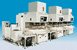 Polishing is the next step in the wafer manufacturing process. Most Prime wafers go through 2-3 polishing steps using progressively finer slurry (slurry is the polishing compound). The polishing is normally done on the frontside of the wafer, but sometimes it is done on both sides. Polishing is done on huge precision machines that are capable of extraordinary tolerances. The systems at the RIGHT have 59" wheels and are made by Speedfam Inc. Prior to final polishing some wafers may receive what is called backside damage, two examples would be bead blast and brush damage. The wafers may also receive a backside coating of Polysilicon, all these treatments are done to the backsides of the wafer for the purpose of Gettering defects(later in the device manufacturing process these backside treatments will draw defects in the Silicon towards the backside of the wafer and away from the frontside where the devices are being built, this is called Gettering). After polishing the wafers are rinsed in DI water and scrubbed to remove any residual slurry compounds from the wafer. Polishing is the next step in the wafer manufacturing process. Most Prime wafers go through 2-3 polishing steps using progressively finer slurry (slurry is the polishing compound). The polishing is normally done on the frontside of the wafer, but sometimes it is done on both sides. Polishing is done on huge precision machines that are capable of extraordinary tolerances. The systems at the RIGHT have 59" wheels and are made by Speedfam Inc. Prior to final polishing some wafers may receive what is called backside damage, two examples would be bead blast and brush damage. The wafers may also receive a backside coating of Polysilicon, all these treatments are done to the backsides of the wafer for the purpose of Gettering defects(later in the device manufacturing process these backside treatments will draw defects in the Silicon towards the backside of the wafer and away from the frontside where the devices are being built, this is called Gettering). After polishing the wafers are rinsed in DI water and scrubbed to remove any residual slurry compounds from the wafer. |
| Final Cleaning: The next step in the process after polishing is a rather intense regimen of cleans and scrubs to remove trace metals, residues and particles from the surface(s) of the finished Silicon wafers. Normally most wafer manufacturers use a final cleaning method developed by RCA in the 1970's the first part of this clean is called SC1 and consists of Ammonium Hydroxide followed by a dilute Hydrofluoric acid clean followed by a DI water Rinse. Next the SC2 clean which consists of Hydrochloric acid and Hydrogen peroxide followed by a DI water rinse. Many companies modify these cleans to make them even more effective. After all this cleaning and rinsing the finished wafers will now go through a front and backside scrub to remove even the smallest particles. |
.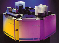 Final sort and inspection: This is one of the last steps in the long wafer manufacturing process. It is here that the wafers either meet or fail the specifications the customers (IC manufacturers) have asked for. There are many specifications the final prime wafers must meet according to agreements made between the customers and the Silicon manufacturer. We will talk about these specifications in a generalized form here, some specifications are tighter, some more relaxed depending on the end user and their requirements. Not including particles and other visual measurements most final sorting of wafers occurs on a automated system like the ADE 9650 pictured at the RIGHT. These compact systems can measure many different parametersincluding Thickness, Bow-Warp, TTV, Site & Global flatness, Type and Resistivity. Final sort and inspection: This is one of the last steps in the long wafer manufacturing process. It is here that the wafers either meet or fail the specifications the customers (IC manufacturers) have asked for. There are many specifications the final prime wafers must meet according to agreements made between the customers and the Silicon manufacturer. We will talk about these specifications in a generalized form here, some specifications are tighter, some more relaxed depending on the end user and their requirements. Not including particles and other visual measurements most final sorting of wafers occurs on a automated system like the ADE 9650 pictured at the RIGHT. These compact systems can measure many different parametersincluding Thickness, Bow-Warp, TTV, Site & Global flatness, Type and Resistivity. Particles, Scratches and haze are normally measured on a system like a Tencor Surfscan 6420 pictured at the LEFT. These systems can sort for pits in the Silicon, tiny scratches and the smallest particles on the best most highly polished Prime wafers. Note: Even the newest particle counters need regular calibration using a traceable particle standard. At the most enhanced viewing levels, the surface of many films (like Silicon Nitride) can be rough or have other defects & features that can show up as particles on a un-calibrated system, even when there is No particulate present. Particles, Scratches and haze are normally measured on a system like a Tencor Surfscan 6420 pictured at the LEFT. These systems can sort for pits in the Silicon, tiny scratches and the smallest particles on the best most highly polished Prime wafers. Note: Even the newest particle counters need regular calibration using a traceable particle standard. At the most enhanced viewing levels, the surface of many films (like Silicon Nitride) can be rough or have other defects & features that can show up as particles on a un-calibrated system, even when there is No particulate present. |
 |
 P-Type wafers are Prime or Test wafers that have Boron as the main dopant. A P+ wafer is heavily doped with Boron <1 Ohm/cm2 (normally will be used as an Epi substrate). A P- wafer is lightly doped with Boron and usually has a resistivity >1 Ohm/cm2 an example would be 5-10 Ohm/cm2. P-type wafers can have a 100 orientation (most common) or a 111 orientation (the 111 substrate is normally used for Bi-polar devices). Note: We do not recommend using 111 material for R & D Etch or lithography purposes Because it breaks into pie shaped pieces when it is cleaved and it is therefore no good for SEM. analysis. P-Type wafers are Prime or Test wafers that have Boron as the main dopant. A P+ wafer is heavily doped with Boron <1 Ohm/cm2 (normally will be used as an Epi substrate). A P- wafer is lightly doped with Boron and usually has a resistivity >1 Ohm/cm2 an example would be 5-10 Ohm/cm2. P-type wafers can have a 100 orientation (most common) or a 111 orientation (the 111 substrate is normally used for Bi-polar devices). Note: We do not recommend using 111 material for R & D Etch or lithography purposes Because it breaks into pie shaped pieces when it is cleaved and it is therefore no good for SEM. analysis. |
 N-Type wafers are Prime or Test wafers that have Phosphorus, Antimony or Arsenic as the main dopant. A N+ wafer is heavily doped <1 Ohm/cm2 (and very rare). The most common N-Type wafer is doped with either Antimony or Phosphorus and has a resistivity >1 Ohm/cm2 (normal for device building would be 2-10 Ohm/cm2). The later being used most commonly for advanced CMOS device fabrication where implanted P-Wells are used. N-Type wafers are Prime or Test wafers that have Phosphorus, Antimony or Arsenic as the main dopant. A N+ wafer is heavily doped <1 Ohm/cm2 (and very rare). The most common N-Type wafer is doped with either Antimony or Phosphorus and has a resistivity >1 Ohm/cm2 (normal for device building would be 2-10 Ohm/cm2). The later being used most commonly for advanced CMOS device fabrication where implanted P-Wells are used. |
. Total Thickness Variation is an important measurement done on Prime wafers at final inspection. It is done on a flatness checking machine like the ADE system pictured above. TTV represents the difference between the minimum and maximum thickness measured on the wafer. A typical number on a good 8" Prime wafer would be < 15 um (of course as you read this the art of wafer polishing is advancing and better and better TTV's are being reported). We have seen "test" wafers with high TTV's and a high Taper reading that look like a wedge! Total Thickness Variation is an important measurement done on Prime wafers at final inspection. It is done on a flatness checking machine like the ADE system pictured above. TTV represents the difference between the minimum and maximum thickness measured on the wafer. A typical number on a good 8" Prime wafer would be < 15 um (of course as you read this the art of wafer polishing is advancing and better and better TTV's are being reported). We have seen "test" wafers with high TTV's and a high Taper reading that look like a wedge! |
 .Site TIR or Total Indicator Reading is a site by site measurement of flatness of a Prime wafer. There are a few ways of taking this measurement Best fit, site Best fit, etc. If you are interested in great optical submicron Photolithography there is only one the Silicon guys will admit is the best way of measuring flatness. That way is Site flatness-Backside referenced measuring a 20x20mm or larger site and each one of these sites must meet <.3 um flatness across each site. Now thats a wafer you can resolve .25-.5 um geometries on, and if it meets this specification on 90-100% of the sites on the wafer you have got a really Great wafer! We are not even going to discuss Global flatness on this page because we think that parameter alone without Site TIR is next to worthless! .Site TIR or Total Indicator Reading is a site by site measurement of flatness of a Prime wafer. There are a few ways of taking this measurement Best fit, site Best fit, etc. If you are interested in great optical submicron Photolithography there is only one the Silicon guys will admit is the best way of measuring flatness. That way is Site flatness-Backside referenced measuring a 20x20mm or larger site and each one of these sites must meet <.3 um flatness across each site. Now thats a wafer you can resolve .25-.5 um geometries on, and if it meets this specification on 90-100% of the sites on the wafer you have got a really Great wafer! We are not even going to discuss Global flatness on this page because we think that parameter alone without Site TIR is next to worthless! |
 Bow & Warp are two important specifications in determining the quality of a wafer at final inspection. First let's discuss Bow, this is the measure of how concave or convex the deformation of the median surface of the wafer at the center point, independent of any thickness variations.In this measurement the wafer is in an unclamped state on the chuck of the measurement system a normal or good Bow number on an 8" Prime wafer would be < 30 um. The easy way to visualize Bow is if you think of the wafer as a bowl turned either upside down or rightside up on a flat surface (convex or concave). Next let's talk about Warp, this measument is also made in an unclamped state. Warp is the difference between the maximum and minimum deviations of the median surface relative to the backside reference plane. Now thats a mouthfull, to simplify things think of warp as the deformation of a wafer kind of like a potato chip, thats the easiest way to explain it. A good Warp number on an 8" wafer would be <20 um. Bow & Warp are two important specifications in determining the quality of a wafer at final inspection. First let's discuss Bow, this is the measure of how concave or convex the deformation of the median surface of the wafer at the center point, independent of any thickness variations.In this measurement the wafer is in an unclamped state on the chuck of the measurement system a normal or good Bow number on an 8" Prime wafer would be < 30 um. The easy way to visualize Bow is if you think of the wafer as a bowl turned either upside down or rightside up on a flat surface (convex or concave). Next let's talk about Warp, this measument is also made in an unclamped state. Warp is the difference between the maximum and minimum deviations of the median surface relative to the backside reference plane. Now thats a mouthfull, to simplify things think of warp as the deformation of a wafer kind of like a potato chip, thats the easiest way to explain it. A good Warp number on an 8" wafer would be <20 um. |
 .Resistivity is very important, if you are trying to make good devices or grow uniform Thermal Oxides. The more uniform the resistivity across the wafer and across the cassette of 25, the more uniform the Thermal Oxide you can grow. Understand that how uniform the resistivity of your start material is directly related to how your Oxide will grow. Most engineers know that Thermal Oxide grows faster in areas of low resistivity (more Dopant) and slower in areas of High resistivity (less dopant) To simplify things think of dopant as fertilizer on your lawn, wherever there is more fertilizer, the grass always grows faster... Right? Thermal Oxide growth works the same way! If the dopant uniformity of the start wafer is good you can expect a good Thermal Oxide. Of course that transforms into terrific gate Oxides and more stable and reliable devices. Ingots can have resistivity problems as well as some wafers. We have seen resistivity changes across a finished wafer of 2-4% and on Epitaxial wafers we have seen radial resistivity vary across a epitaxial wafer with a median resistance of 3 -20 Ohm/cm2 up to 15% across the wafer! As you can see epitaxial wafers are not always a good choice for uniform thermal Oxides. .Resistivity is very important, if you are trying to make good devices or grow uniform Thermal Oxides. The more uniform the resistivity across the wafer and across the cassette of 25, the more uniform the Thermal Oxide you can grow. Understand that how uniform the resistivity of your start material is directly related to how your Oxide will grow. Most engineers know that Thermal Oxide grows faster in areas of low resistivity (more Dopant) and slower in areas of High resistivity (less dopant) To simplify things think of dopant as fertilizer on your lawn, wherever there is more fertilizer, the grass always grows faster... Right? Thermal Oxide growth works the same way! If the dopant uniformity of the start wafer is good you can expect a good Thermal Oxide. Of course that transforms into terrific gate Oxides and more stable and reliable devices. Ingots can have resistivity problems as well as some wafers. We have seen resistivity changes across a finished wafer of 2-4% and on Epitaxial wafers we have seen radial resistivity vary across a epitaxial wafer with a median resistance of 3 -20 Ohm/cm2 up to 15% across the wafer! As you can see epitaxial wafers are not always a good choice for uniform thermal Oxides. |
 Defects in Silicon are one of the principle causes for rejection of Silicon wafers both by the large Silicon manufacturers and the IC manufacturers. A lot of the time if you buy wafers from a Silicon Vendor and not a manufacturer they might be called "Prime wafers", but chances are they have some faults. Most likely they have been rejected by some Fab or the Wafer manufacture for one thing or another, and if you can find out what for, you are way ahead of the game. Remember though this is not a bad thing, most of these wafers are perfectly fine for most tool R & D uses and they are able to be sold for reasonable prices. True prime wafers that meet all the specs and are suitable for device manufacture are very expensive! So smile when you get a good price on Prime and you get a good wafer with very few defects. There are many defects associated with Silicon wafers and most are caught at the Silicon Manufacturer, some are not. Wafer defects range from pits in the Silicon surface and tiny scratches, to things that are Hidden from view, buried below the Silicon surface like the picture at the RIGHT of Copper Precipitates (a common defect). Found just below the Silicon surface by means of a SIRTL etch for 60 sec. This defect exhibits a crows foot like appearance and would cause a bad Gate Oxide over this region, causing a failed device(s). If this defect was under a few points on your 49 point Thermal Oxide Measurement map, you would definitely see non-uniform Oxides in these areas (Thermal Oxide growth can accelerate or decelerate over defects in the Silicon). There are many Hidden defects in Silicon wafers and to date no one has made a perfect one. Perhaps someday when they grow ingots on the Space station we will get Silicon with zero defects but until then, the major Silicon manufacturers back on Earth are turning out some incredible Silicon Wafers! Defects in Silicon are one of the principle causes for rejection of Silicon wafers both by the large Silicon manufacturers and the IC manufacturers. A lot of the time if you buy wafers from a Silicon Vendor and not a manufacturer they might be called "Prime wafers", but chances are they have some faults. Most likely they have been rejected by some Fab or the Wafer manufacture for one thing or another, and if you can find out what for, you are way ahead of the game. Remember though this is not a bad thing, most of these wafers are perfectly fine for most tool R & D uses and they are able to be sold for reasonable prices. True prime wafers that meet all the specs and are suitable for device manufacture are very expensive! So smile when you get a good price on Prime and you get a good wafer with very few defects. There are many defects associated with Silicon wafers and most are caught at the Silicon Manufacturer, some are not. Wafer defects range from pits in the Silicon surface and tiny scratches, to things that are Hidden from view, buried below the Silicon surface like the picture at the RIGHT of Copper Precipitates (a common defect). Found just below the Silicon surface by means of a SIRTL etch for 60 sec. This defect exhibits a crows foot like appearance and would cause a bad Gate Oxide over this region, causing a failed device(s). If this defect was under a few points on your 49 point Thermal Oxide Measurement map, you would definitely see non-uniform Oxides in these areas (Thermal Oxide growth can accelerate or decelerate over defects in the Silicon). There are many Hidden defects in Silicon wafers and to date no one has made a perfect one. Perhaps someday when they grow ingots on the Space station we will get Silicon with zero defects but until then, the major Silicon manufacturers back on Earth are turning out some incredible Silicon Wafers! |
| . Epitaxy: The growth of a single crystal Silicon layer on the front side of the wafer (polished side) is something Silicon manufactures do all the time. This is a very difficult process and is prone to many defects. It is normally part of the Silicon manufacturing process, but it is also done at the IC manufacturing facilities. For this reason we will discuss this CVD film in more detail in another article. |
| If you read your way down this page, you know a lot more about Silicon wafer manufacturing than most people that work in the Silicon Valley! If you scrolled down the page looking at the pictures maybe you're interested enough now to go back up to the top of the page and read your way down this time, and you might learn something too! |
| .If you would like more information on Silicon wafer processing, talk to a Silicon manufacturer or give one of our process engineers a call (800) 533-8820 or e-mail us at Process Specialties Inc. |
   |
© 1997 Process Specialties Inc. |
Wednesday, February 15, 2017
Silicon Information
Silicon Information
Subscribe to:
Post Comments (Atom)
No comments:
Post a Comment